|
|
|||||||||||||||||||||||||||||||||||||||||||||||||||||||||||||||||||||||||||||||||||||||||||||||||||||||||||||||||||||||||||||||||||||||||||||||||||||||||
| Upcoming Features... personalized main page, discussion forum, workbench calculator... | |||||||||||||||||||||||||||||||||||||||||||||||||||||||||||||||||||||||||||||||||||||||||||||||||||||||||||||||||||||||||||||||||||||||||||||||||||||||||
|
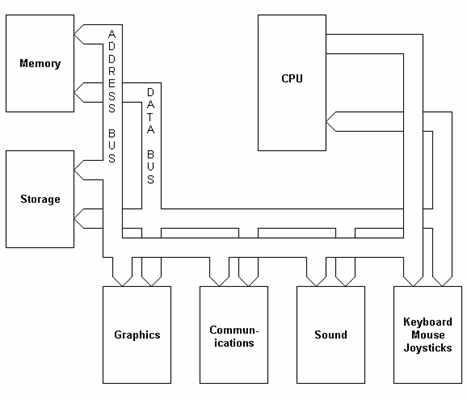
How to Control Electronic Circuits Using a Computer and the BASIC Programming Language by Donald J. Bartley Introduction There is nothing more satisfying then writing a computer program, executing it, and watching it run; hopefully faultlessly. It’s akin to the same feeling you get when you create a new electrical circuit and watch it operate for the first time. It's that feeling of creation. Seeing something, that was once a thought, being manifested into the material world. Saying, 'this didn't exist until I created it'. Electrical engineering and computer science is all about that; bringing something into existence purely through will power and thought. The two disciplines are separate and are taught differently, each having its own college and/or university degree. However, combining the two disciplines together is where the real fun begins. Design a circuit, build it, connect it to a computer, write a program to transfer data to and from the circuit, run it and watch it all work; the two disciplines married together and working in harmony. It's really quite simple since a computer is just an electrical circuit itself. The circuit connected to the computer is just an extension of it. At that point you just need to write a computer program to talk with that 'extension'. This paper will guide you through how to do just that. We'll review a simple computer system and how it works. Then we'll take a look at the BASIC programming language and the statements that it has that will allow us to 'talk' with the external circuitry. Next we'll take a look at how to 'interface' your electronic circuit to a computer so that it works in 'harmony' with the rest of the computer. Lastly, we'll end with two examples which show simple experiments you can do to practice writing and reading data from your circuit. Computer Systems The figure below shows a simple computer system and its connections. Keep in mind that this is a just a general overview. The circuitry inside a computer can get much more complicated than this but for the purposes of this discussion this general overview will suffice.
The computer above has all the basic components. It has memory for program and data storage, it has a storage device for saving user programs, a graphics interface for connection to a video screen, a communications interface so data can be transferred between it and other computers, a means of generating sounds, user interface devices such as a keyboard, and lastly the brains of the operation the Central Processing Unit or CPU. The first thing that becomes clear is that all these components are connected together using two busses, an address bus and a data bus. These two busses combined constitute the 'bussing system' of the computer and they are the main pipelines for all data transfers inside the computer. Here is how it works. The concept of an address is not new to any us, we each have a street address or a post office box number where mail can be sent to us. The address uniquely identifies us from our neighbors. This system works the exact same way in a computer system. Each of the components above has a unique address. When the CPU wants to send or receive data from the memory it sends out the unique address for the memory on the address bus. This tells the memory that the data bus is now available to it. Any data put on the data bus from the CPU is for the memory and any data the memory wants to send to the CPU can be put on the data bus. All the other components in the computer system are attached to the address bus and since the address is not theirs they stay 'disconnected' from the data bus so as not to interfere with the transfer of data between the CPU and the addressed device. With the common address bus the CPU can 'select' one component at a time for data transfer. This allows the CPU to know exactly where data is being sent to and where it is being received from. The common address bus keeps the system 'organized' and keeps multiple components from using the data bus at the same time. So how many addresses are there? Well, much like the houses on a street there can only be a certain amount. The amount of houses on a street is dictated by the size of the street. The amount of addresses on an address bus is dependant on how many bits the address bus is comprised of. Just a quick refresher course about digital logic; a bit is the smallest piece of information in a digital system. A bit represents a single piece of information and it can only have two states, either logic low (represented by 0) or logic high (represented by 1). Four of these bits can be used together to form a nibble, eight of them together make a byte, and 16 of them become a word. The amount of data that can be represented by these combinations is figured out through a simple formula, 2 raised to the power of X or 2X; where X represents the number of bits. For a nibble (4 bits) the formula gives us 24=16. This means that a nibble can represent 16 numbers so starting at 0 that gives us 0 to 15. A byte (8 bits) gives us 28=256 which means the numbers 0 through 255 can be represented. For a word (16 bits) we get 216=65,536 so the numbers 0 through 65,535 can be represented with a word. For the purposes of this discussion were going to say that the address bus of our computer system in Figure 1 has a 16 bit address bus and an 8 bit data bus. With a 16 bit address bus this means that the CPU can address up to 65,536 unique locations in the computer; or 64K. In computer terms K equals 1,024 so 64K is 64x1,024 which equals 65,536. There is one more important signal to discuss that is not in the diagram of Figure 1. It is called the read/write line. The read/write (R/W) line is the traffic cop of the data bus. This signal indicates whether data is being written to or read from the CPU. When the R/W line is logic high (1) the data bus is in read mode. This means that the CPU is in input mode and data is being written to it. When the R/W line is logic low (0) the data bus is in write mode. This means that the CPU is in output mode and data is being read from it. When a logic low (0) is present on the R/W line any logic device connected to the data bus should make all its output lines high-impedance. This means that the pins connected to the data bus need to have a high input resistance so that the CPU is free to drive the data bus lines without interference from any other component. In some computer system the R/W line is a single line, like as we discussed here. In other systems the R/W signal is broken up into two lines; a read line and a write line. In either case the result is the same. This signal is responsible for direction control. In the section called 'Interfacing to a Computer System' we'll learn how to use all this information together and connect our own circuits to a computer. But with a fundamental understanding of how a computer works now under our belt lets take a look at programming. The BASIC Programming Language A programming language is used by a user to 'instruct' the computer on what the user needs the computer to do. The CPU in a computer only understands one language; it is commonly referred to as machine language. Programming in machine language can be a difficult task and it doesn't lend itself to being easy to understand. Because this language is directly translatable by the CPU it is called a 'Low Level Language'. Programming languages such as BASIC, C, and Fortran are called 'High Level Languages'. These languages require an interpreter or compiler to operate. The interpreter or compiler changes the syntax of the language and converts it to machine code so that it can be understood by the CPU. Because these high level languages remove the programmer from the execution semantics of a computer system it makes the process of developing a program simpler and more understandable. For our purposes we will be using the BASIC language. What is BASIC? BASIC (an acronym for Beginner's All-purpose Symbolic Instruction Code) refers to a family of high level programming languages. The original BASIC was designed in 1963, by John George Kemeny and Thomas Eugene Kurtz at Dartmouth College. At the time, nearly all use of computers required writing custom software, which was something only scientists and mathematicians tended to do. BASIC was intended to address the complexity issues of older languages with a new language design specifically for a new class of computer users — that is, a less technical user who did not have the mathematical background of the more traditional users and was not interested in acquiring it. The eight design principles of BASIC were:
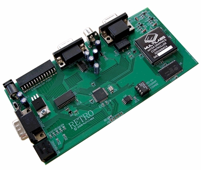
BASIC remains popular to this day in a handful of highly modified dialects and new languages based on the original BASIC. BASIC is being used in these examples because it is easy to understand and learn. This will allow more concentration to be put on interfacing and using a computer to control electronic circuits instead of learning to program. Once the fundamentals of these experiments are well understood the reader is free to take the information and expand upon it using different techniques and methods. The computer system that will be used in these experiments is the Retro computer system from Multilabs.
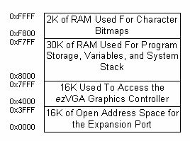
Figure 2 Retro is simple to use, provides a built-in BASIC language interpreter, and has easy access to the address and data buses; everything that is needed to provide a simple and straightforward learning environment. The BASIC dialect that is discussed in this paper is in reference to the Retro computer system. It is assumed that the reader has a general knowledge of the BASIC language already. To get a better grasp of the BASIC language and how to use Retro it is recommended that you download the User Manual from Multilabs' website. This manual will give you detailed information about BASIC, its syntax, structure, and how to use it. BASIC contains two statements that will be integral to these experiments, they are PEEK and POKE. PEEK returns an integer value which is read from a location on the address bus. The syntax for PEEK is: PEEK(<expression>). The expression is the address bus location. The PEEK statement can be used to read a single byte of data from an external device connected to the computer. An example of the PEEK statement in BASIC is: PRINT PEEK(15342) The POKE statement is used to write a byte value into a given address location. The syntax for POKE is: POKE <expression>,<expression>. The address is the first expression and the value to be written is the second expression. The POKE statement can be used to write a single byte of data to an external device connected to the computer. An example of the POKE statement in BASIC is: POKE 14211,24 Using these two statements along with some other BASIC statements you'll be controlling your own electronic circuits with a computer in no time. Interfacing to a Computer System There are two things you need to interface to a computer's bussing system. First, you need access to the address bus, data bus, and the supporting read/write lines. Secondly, you need what is known as a memory map of the computer system. A memory map shows you how the addresses are used in the computer system. For example, here is the memory map for the Retro computer system:
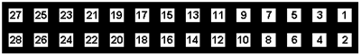
Table 1 This computer has a 16 bit address bus and Table 1 shows all 64K of address space summed up. The addresses shown on the left hand side are represented in hexadecimal format. If you’re not familiar with it don’t worry. Here are the decimal conversions: 0xFFFF = 65535 0xF800 = 63488 0xF7FF = 63487 0x8000 = 32768 0x7FFF = 32767 0x4000 = 16384 0x3FFF = 16383 0x0000 = 0 As you can see program storage starts at address 32768 and expands upward towards the character storage area. Addresses 16384 through 32767 are dedicated to the graphics system. Addresses 0 through 16383 are all yours. These can be used with the expansion port to access and control external circuits. The expansion port is used to access the system busses and support lines. Here is the pin-out for Retro's expansion port:
Figure 3
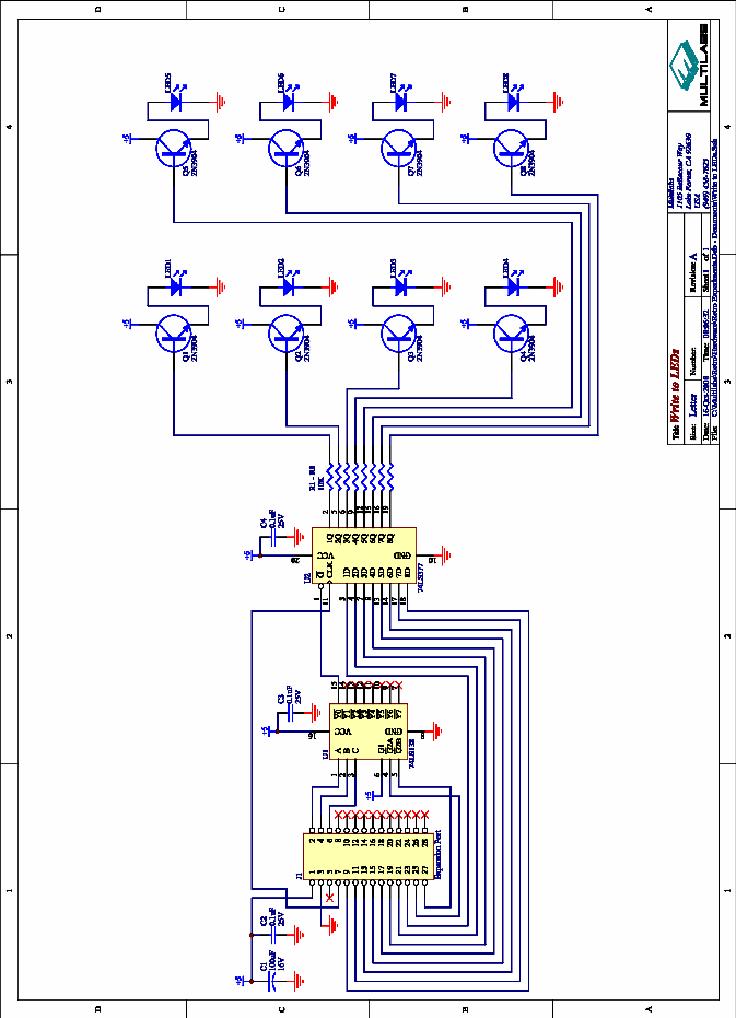
Table 2 Before going any further it is important to go over a few rules. First and foremost the expansion port gives you access to the data and address buses of Retro. This goes for any computer system when connecting to its bussing system. These buses are the "central nervous system" of any computer. If one or both are damaged the system fails. When you are connected to these busses you are connected to the CPU, graphics processor, memory, etc. Extreme caution must be taken while connected to these busses. Any short circuits, power surges, illegal writes to the data bus, etc. may damage one or all of these parts and damage the computer to where it is no longer useful. If the example experiments are followed and the rules of addressing and data transfer are observed there will be no problems and everything will work solid for as long as you would like it to. To avoid shorts do not work on your circuit while it is connected to a computer and make sure all your electrical connections are sound. Proper practices in design and construction will ensure that this will be a fun experience. I, the author, know this from first hand experience. I blew out my first computer playing with its user port. Four of the chips, including the CPU, were blown and the computer was destroyed. Since then I’ve connected countless circuits to computers of all kinds with no problems. To was a hard way to learn the rules. As discussed before the address bus of Retro is 16 bits which gives it 65536 unique addresses. The 16 bits are labeled A0 through A15. A0 is the lowest bit and A15 is the highest bit. From the memory map in Table 1 we see that the RAM takes up the upper 32K of address space. This means that when bit A15 of the address bus is logic high (1) then the RAM is selected. Address lines A0 through A14 are used to select which memory location data is written to/read from in RAM memory. Address line A15 sole purpose is to select/enable the RAM chip and make sure that all other devices connected to the bus system are disabled so that the RAM has control over the data bus. When a logic device is unselected/disabled it should make all its output lines high-impedance. This means that the outputs are turned off and a high resistance is seen at the output pins. This brings us to expansion port rule number #1: When address line A15 is logic high (1) any device connected to the data bus must be disabled and have high-impedance outputs. Continuing to look at the memory map we see that the graphics controller is located in the high 16K of the lower 32K of address space. This means that when bit A15 of the address bus is logic low (0) and A14 of the address bus is logic high (1) then the graphics controller is selected. Address lines A0 through A13 are used to select which memory location data is written to/read from. Address lines A15 and A14 sole purpose is to select/enable the graphics chip and make sure that all other devices connected to the bus system are disabled so that the graphics chip has control over the data bus. This brings us to expansion port rule number #2: When address line A14 is logic high (1) any device connected to the data bus must be disabled and have high-impedance outputs. From the first two rules we can surmise that if either A15 or A14 are logic high (1) then any devices connected to the expansion port must be disabled. In other words, both A15 and A14 must be logic low (0). When they are both logic low (0) that means the lower 16K of the lower 32K of address space is selected and from our memory map we see that this is where the expansion port comes in. This lower 16K is unused by anything in the Retro computer system. So when A15 and A14 are both logic low (0) the data bus is up for grabs. We discussed the read/write (R/W) line in a pervious section. To recap, the R/W line indicates whether data is being written to or read from the CPU. When the R/W line is logic high (1) the data bus is in read mode. This means that the CPU is in input mode and data is being written to it. When the R/W line is logic low (0) the data bus is in write mode. This means that the CPU is in output mode and data is being read from it. This brings us to expansion port rule number #3: When the R/W line is logic low (0) any device connected to the data bus must have high-impedance outputs. At this point we know to monitor address lines A15 and A14 along with the R/W line. From these three we can tell if the data bus is free and what direction the data is flowing from the CPU. The last step is learning how to use address lines A0 through A13. To take advantage of all these addresses you need a logic device called an 'address decoder'. Take the 32K RAM memory that is part of Retro as an example. The RAM memory is enabled through address line A15. Address lines A0 through A14 are used to select which of the 32,768 memory locations is used for the read/write operation. To do this the RAM memory comes with a built-in 'address decoder' that turns those 15 address lines into a single signal for each memory location. While this takes a lot of logic to accomplish there are some easy ways to do this with simple logic gates and decoder chips. One simple logic device is called a decoder. They come in 2-line to 4-line, 3-line to 8-line, and 4-line to 16-line packages just to name a few popular ones. In the TTL logic series these chips are 74LS139, 74LS138, and 74LS154 respectively. With a 2-line to 4-line decoder 2 address lines are used to select 4 devices. The 3-line to 8-line decoder uses 3 address lines to select 8 devices. A 4-line to 16-line decoder monitors 4 address lines to select 16 devices. If you look at datasheets for these devices you’ll see the logic that is used to decode the address lines and how complex it can get. It is far easier to use one of these devices then to use discrete logic. While in write mode (data is being written from the CPU) the levels of each data bit are roughly 5V for logic high (1) and 0V for logic low (0). In read mode (data is being written to the CPU) the logic levels outputted from your device must be observed. The central processor uses Schmitt Trigger input buffers. A Schmitt Trigger is a logic circuit that uses a wide gap between the logic high (1) and logic low (0) input voltages in an attempt to keep noise at the input from creating false data. This wide gap between the two voltages is called 'hysteresis'. This means that logic high (1) must be greater than 4V and a logic low (0) must be lower than 1V. Some devices may fall outside of these parameters and should be avoided. Refer to the datasheet for each logic device you are going to use to ensure that these voltage levels can be obtained. For each computer system there should be documentation that indicates what the minimum and maximum input logic voltages should be. These should always be closely observed. In the next two examples we’ll tie it all together and give you a chance to try it all out. These examples show how to apply the rules for monitoring when the data bus is available, how to monitor direction of the data flow, and how to address different devices with the address lines. Experiment #1 – Controlling LEDs This first example will demonstrate how to write data through the expansion port. For this, we’ll use LEDs to display the data. Let’s walk through the schematic on the next page and apply what has been presented so far.
The expansion port is represented by J1. In this example we won’t use all the lines available, just the ones necessary to get us started. The expansion port is equipped to supply +5VDC, 100mA to your projects. If more power is needed then an external supply will have to be used. But 100mA is enough for this small experiment. Note that there are two capacitors connected close to the power line. When using the expansion port not only are you connected to the buses of the system but you are also connected to the power system of Retro as well. Any noise your projects generate can be transmitted into Retro through the power bus. It is a good practice to use decoupling capacitors and filter capacitors no matter which computer system you are connecting to. You’ll see that each logic chip has a decoupling capacitor located near it and the power bus has a decoupling and filter capacitor near the expansion port. Too much noise introduced into Retro may cause improper operation; this should be monitored. The first chip in the system is the decoder that was previously discussed; the 74LS138. On the address side of the chip inputs A, B, and C are connected to address lines A0, A1, and A2 respectively. Inputs G2A and G2B are connected to address lines A14 and A15 respectively. Input G1 is not used and is tied high. All three inputs G1, G2A, and G2B are used to select the chip. In order for the chip to be selected G1 must be logic high (1), G2A must be logic low (0), and G2B must be logic low (0). If these conditions are not met all eight outputs will remain logic high no matter what data is present on A, B, and C. This satisfies the first 2 rules about using the expansion port, both address lines A15 and A14 must be logic low (0). Since G1 is permanently tied logic high (1) address lines A15 and A14 determine when this chip is selected. They both have to be logic low (0) for that to happen. So what happens when both address lines A15 and A14 are logic low (0)? The chip is selected and the three address inputs A, B, and C determine which of the three outputs are active. On the 74LS138 an output is said to be active when it is outputting a logic low (0) signal. Remember, when the chip is not selected, all outputs are logic high (1) no matter what. In this experiment we are only monitoring output Y0. This output is active when all three address inputs are logic low (0). Refer to the following truth table:
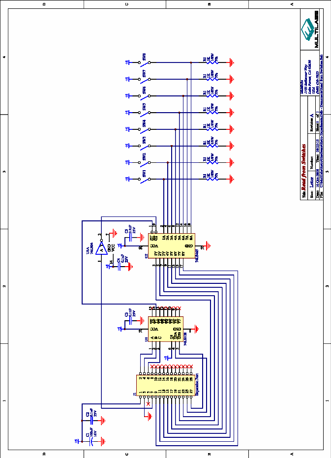
Table 3 Looking at the schematic you’ll see that output Y0 is connected to the enable line of chip U2. This chip is a 74LS377 which is an Octal D-Type Flip Flop storage register. This chip becomes enabled when a logic low (0) is present on its enable pin. The input data lines, 1D through 8D are connected to the data bus of Retro. D0 is connected to 1D, D1 to 2D, and so forth. The R/W line is connected to the clock input of the chip. In this case rule #3 does not apply. If you remember, this rule stated that when the R/W line is low (0) all devices with data outputs are to go high-impedance. In this case the 74LS377 does not have any data output lines that are connected to the expansion port. Only data inputs are connected; but in this case the R/W line still serves an important role. If you remember the previous discussion about the R/W line you’ll remember that it goes logic low (0) while data is being written from the CPU. In this case we’re going to use the R/W line as a data clock. The 74LS377 latches the data that is present at its inputs on the rising edge of the clock pin. The R/W line will go low (0) during the write and then return to logic high (1). When this happens the data will be latched into the storage register. The data will then be permanent even after the chip, and even the entire circuit, is disabled by the address lines. Data has now been written from the expansion port to a specific address. Seeing is believing, build the circuit and give it a try. These parts are all readily available from many electronics distributors, both local and online. Once you have it built try this program: 10 FOR L=0 TO 255 20 POKE 0,L 30 FOR T=1 TO 2500:NEXT 40 NEXT 50 END If everything was built correctly you should see the LEDs do a binary count in about ¼ second increments. Want to see addressing at work? Change line 20 to POKE 1,L and re-run the program. Nothing happens does it? This is because you are now addressing location 1 which keeps the storage register deselected. Now try this. Change line 20 to POKE 8,L and re-run the program. Suddenly its working again, but wait, we’re using address 8 and not 0 so how is that possible? If you look at the schematic you’ll see we’re only monitoring address lines A0 through A2. With address 8 A3 is logic high (1) and A0 through A2 are all logic low (0). So to the 74LS138 it looks like address 0. In order to expand upon this you would need to add logic circuitry that monitored address lines A3 through A13 and would keep the 74LS138 deselected if any of them were logic high (1). Remember from the schematic that G1 is permanently tied high? Well, put A3 through A13 into a NOR gate so that if any of them are logic high (1) the output of the NOR gate would be logic low (0). Since G1 has to be logic high (1) in order for the chip to be selected tie the output of the NOR gate to G1 and you got it. See how it works? Let’s try a read through the expansion port now. Experiment #2 – Reading Switches Take a look at the schematic on the next page and you’ll see quite a few similarities.
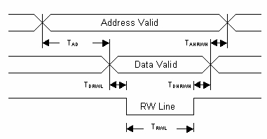
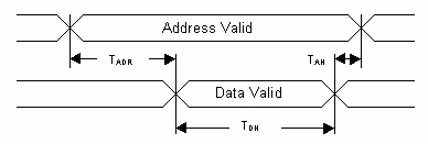
Our front end looks just the same. J1 is the expansion port, U1 is used to select devices based on the address lines, and all parts are filtered for noise. The difference comes in with U2 which is a 74LS465 Octal Buffer with 3-State Outputs. First notice that one of the enable lines of U2 is connected to Y1 of our U1 address decoder. In the previous experiment we used Y0. This means that the active address will be 1 instead of 0. The other enable line is connected to the inverter U3A. This goes with rule #3 which stated that when the R/W line is logic low (0) anything connected to the data bus with outputs needs to go high-impedance. Both of the enable lines of U2 need to be logic low (0) for the chip to be enabled. If the chip is not enabled than the outputs (1Y through 8Y) go high-impedance. This second enable line is used to monitor the R/W line. Since we need the enable line of U2 to go logic high (1) when the R/W line is logic low (0), we use an inverter to accomplish this. So now any POKE to address 1 will cause U2 to be disabled. The rest of it is pretty straight forward. The outputs of U2, 1Y through 8Y, are connected to the data bus D0 through D7 respectively. The inputs of U2, 1A through 8A, monitor the switches. When a switch is open the input is logic low (0). When the switch is closed logic high (1) appears on the input. Again, seeing is believing, build the circuit and give it a try. As with the previous circuit these parts are all readily available from many electronics distributors, both local and online. Once you have it built try this program: 10 CLS 20 PRINT PEEK(1) 30 GOTO 20 If everything is correct you’ll see numbers being printed on the screen. Changing the status of the switches should change the numbers. All switches open will be 0 and all switches closed will be 255. Essentially, you’re reading the binary representation of the eight switches. Hitting the <Esc> key will stop the program. Change line 20 to PRINT PEEK(0) and re-run the program. Random numbers appear that do not follow the switches. That is because we switched the addressing of this experiment to address 1 through our address decoder. As before, if you change line 20 to PRINT PEEK(9) the program will work just fine. As discussed before, this is because were not monitoring address lines A3 through A13. But from our previous discussion we already know how to correct this with a simple NOR gate. Congratulations! You know how to address different circuits through the expansion port and read/write data. At this point let your creativity run wild. Instead of transistors running LEDs they can run motors. Instead of switches you can read data from analog to digital converters. There are so many possibilities. Did you notice that the two experiments presented above can be connected together? One is address 0 and one is address 1, it can be made into one complete circuit. Write a program that reads the switches and transfers the data to the LEDs so that the LEDs follow the switch changes. There is one more piece of information that you’ll need for the expansion port. Address and data bus timing. Timing Diagrams Everything in a computer is clocked from the CPU. This means that there is a certain 'window' in which data can be read from and written to any device in the system or any circuit connected to any expansion port. After the address lines are stable this starts the countdown. The data to be written will only appear for a certain time and any data to be read has to appear on the data bus before a certain time expires. For the most part, most logic chips on the market will be able to keep up with these speeds. The 74LS chips presented in the two experiments are plenty quick enough. This data will be presented to you for your reference so any chip that you may be using can be checked to make sure it meets the timing requirements. There are two timing diagrams for the Retro computer system. One for writing data (POKE statement) and one for reading data (PEEK function).
Figure 6 - Data Write Timing Diagram
Table 4 - Data Write Timing Table
Figure 7 - Data Read Timing Diagram
Table 5 - Data Read Timing Table Conclusion: You have been presented with a fundamental overview of computer bussing systems, how they work, how to connect to them, and how to control them through computer programs. Access to the bussing systems of modern computers has become more and more limited with time. However, there are a number of embedded and hobbyist computers on the market today that still have these components readily available. Embedded programming and devices such as microcontrollers have taken over as the controllers for electronic circuits but computers still have some advantages depending on the application. Donald J. Bartley
|
|||||||||||||||||||||||||||||||||||||||||||||||||||||||||||||||||||||||||||||||||||||||||||||||||||||||||||||||||||||||||||||||||||||||||||||||||||||||||
|
WorkbenchFun.com is a trademark of electricalfun.com © 2008 Project Submission Guidelines |